In this article (4)
The Equipment Layer Is the Bottleneck: Applied Materials' New Tools Show Where 3D Chip Scaling Gets Stuck
Key Takeaways
- The real constraint in 3D chip scaling is now process equipment, not transistor design: tools that cannot deposit or etch precisely inside deep narrow structures block entire architecture generations.
- Molybdenum is emerging as a platform-level material across both GAA logic and 3D NAND memory, and the tools to deposit and selectively etch it are already shipping in production fabs.
- Understanding ALD, selective etch, and materials properties at nanoscale is essential for anyone studying semiconductor engineering, because these are the mechanisms behind every density and performance gain.
Two new systems launched June 15, 2026 reveal that precision deposition and selective etch, not transistor design, are now the active constraints on vertical chip scaling.
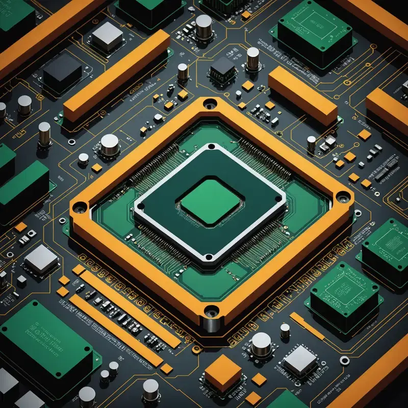
Picture a skyscraper being built one atom at a time, where each floor must be perfectly level before the next can go on, and the elevator shaft runs straight through every floor without touching the walls. That is roughly what it means to manufacture a modern 3D NAND chip, and it is getting harder to pull off with every additional story added. The challenge is not a shortage of clever chip designers. It is the physical reality of depositing and etching materials inside structures so deep and narrow that conventional tools simply cannot reach the bottom without making a mess on the way down.
What Applied Materials Actually Launched, and
Why the Date Matters On June 15, 2026, Applied Materials introduced two new chipmaking systems aimed squarely at this problem, according to the company's official press release published on GlobeNewswire. The first is the Centris Spectral SiN ALD system, which uses microwave plasma technology to deliver uniform silicon nitride deposition inside challenging 3D structures. The second is the Producer Selectra Mo Etch system, which selectively removes molybdenum for wordline separation to enable 3D NAND scaling. Per the same GlobeNewswire release, both systems are already in use by leading logic and memory chipmakers for advanced node manufacturing. The fact that these tools are shipping into production fabs rather than sitting in a demonstration lab is the detail worth pausing on. This is not a roadmap slide. It is an installed capability. The timing is directly tied to AI compute demand: as BriefGlance summarizes in its event coverage, the semiconductor industry is accelerating its transition to advanced 3D device architectures driven by demand for AI compute, with these systems designed to overcome critical scaling barriers and enable continued 3D scaling with better device performance and manufacturability. The architectures in question include gate-all-around (GAA) transistors and high-layer-count 3D NAND, per the GlobeNewswire release.
The Physics of Going Vertical, and Why Old Tools Fail To understand
why these two tools matter, you need a mental model of what high-aspect-ratio 3D structures actually demand from a deposition or etch process. Aspect ratio is the ratio of a structure's depth to its width. When that ratio climbs, you are asking a process gas or plasma to travel a very long way down a very narrow tunnel and then do precise chemistry at the bottom without disturbing the walls on the way. Atomic layer deposition, or ALD, addresses the deposition side of this problem by building films one atomic layer at a time, cycling between precursor gases to achieve thickness control that conventional chemical vapor deposition cannot match in confined geometries. The Centris Spectral SiN ALD system uses microwave plasma to energize that process, which is significant because microwave plasma generates a more uniform, lower-damage plasma than traditional radio-frequency approaches, helping the chemistry stay consistent even deep inside a narrow structure. Silicon nitride is the specific material being deposited here, and it matters because SiN is widely used as a spacer and insulating layer in both GAA transistor stacks and 3D NAND cell arrays, according to Applied Materials' GlobeNewswire announcement. The etch side of the equation is where molybdenum enters the story, and it is the more counterintuitive half. Molybdenum has been emerging as a preferred metal for transistor contacts and, critically, for the wordlines in 3D NAND, replacing tungsten in some applications because of its lower electrical resistance at small dimensions. But molybdenum is only useful if you can remove it with surgical precision from the places you do not want it, without attacking the surrounding silicon nitride or oxide layers. According to Applied Materials' official investor relations release, the Producer Selectra Mo Etch system delivers exactly that: selective molybdenum removal for wordline separation, which is the step that electrically isolates each layer of a 3D NAND stack from its neighbors.
Why the Equipment Layer Is
the Constraint Now Here is the thing chip keynotes rarely say out loud: at a certain point in the scaling roadmap, the limiting factor stops being what you can design and starts being what you can physically deposit or remove without wrecking everything adjacent to it. The semiconductor industry has been living in that regime for several years, and the launch of these two tools is a clear signal that the equipment layer is actively constraining what chipmakers can build, not just enabling it. This matters for learners because it reframes where innovation is actually happening. When you read about a new chip architecture, GAA transistors replacing FinFETs, or higher-layer-count NAND, the invisible prerequisite is a set of process tools capable of executing that architecture at volume. According to the GlobeNewswire release, the new systems are designed to help chipmakers deliver higher performance, improved energy efficiency, and better manufacturing yield. Those three outcomes do not appear automatically from a clever schematic; they require process equipment that can hold tolerances inside geometries that are genuinely difficult to visualize at human scale. The competitive context is worth noting too. BriefGlance flags that how competitors like Lam Research and Tokyo Electron respond to these launches is an active open question, which tells you this is a contested space where the equipment vendors are competing as intensely as the chipmakers themselves. Applied Materials is not alone in this race, and that competition is ultimately good for the industry because it accelerates the tool development that makes the next generation of chip architectures manufacturable.
What This Means
for Anyone Learning About Semiconductors If you are studying electronics, materials science, or computer engineering, the story of these two tools is a masterclass in why the physical layer of technology never stops mattering. ALD, plasma chemistry, selective etch, and materials properties like electrical resistance at nanoscale dimensions are not obscure specializations. They are the mechanisms by which every transistor count increase and every memory density improvement actually gets realized in silicon. The molybdenum story is particularly worth following. As Applied Materials noted in a February 2026 YouTube announcement about earlier transistor and wiring innovations, the Centris Spectral Molybdenum ALD system had already been introduced to replace tungsten contacts with molybdenum at 2nm and beyond, lowering electrical resistance at the critical link between transistors and the copper wiring network. The June 2026 Producer Selectra Mo Etch launch extends molybdenum process capability to the memory domain, suggesting the material is becoming a broader platform choice rather than a one-off substitution. Watching how molybdenum process tools proliferate across logic and memory nodes over the next few years will tell you a great deal about where materials engineering is headed at the atomic scale.