In this article (4)
Google Just Bet Three Million TPUs on Intel Foundry. Here's Why That's the Signal Everyone Missed.
Key Takeaways
- Google's order of 3 million TPUs from Intel for 2028 followed months of engineering validation, not a marketing deal. Test before you commit.
- Advanced packaging, specifically Intel's EMIB bridging compute dies and HBM, is the technical capability that earned Intel this business.
- Nvidia evaluating Intel's 18A node for multi-die GPUs signals Intel Foundry has cleared a credibility threshold, even if no order exists yet.
Alphabet's 2028 chip order is a quiet but consequential vote for a second advanced-node supplier, and Nvidia may be watching closely.
Three million is a big number. It is the kind of number that shows up in a procurement order, gets buried in a supply chain report, and then quietly rewrites the foundry landscape for the rest of the decade. According to Tom's Hardware, Google has placed an order for Intel to build more than three million of its TPUs in 2028, after months of testing Intel's advanced packaging. That last detail is the one worth holding onto: months of testing. This wasn't a strategic press release. It was an engineering decision.
What Google Actually Ordered, and
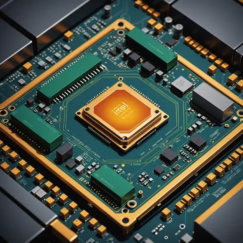
Why the Packaging Detail Matters TPUs, or Tensor Processing Units, are Google's custom-designed accelerator chips, purpose-built to run the matrix math that underlies machine learning workloads. They are not general-purpose processors. Google designs them in-house, which means the choice of who manufactures them is entirely Google's to make. For years, the default answer for anyone building at advanced nodes was TSMC, and for good reason: TSMC has the yields, the capacity, and the track record. So when Tom's Hardware reports that Google booked Intel for more than three million of these chips, with delivery targeted for 2028, the interesting question is not "how many" but "why Intel, and why now." The answer lives in the phrase "advanced packaging." Tom's Hardware notes that the order came after months of testing Intel's advanced packaging capabilities, and separately that SK Hynix is testing Intel's EMIB packaging for HBM integration. EMIB, or Embedded Multi-die Interconnect Bridge, is Intel's technology for connecting multiple chiplets on a single package with high bandwidth and low power overhead. Think of it like this: if a single monolithic chip is a single kitchen doing everything, a multi-die package connected by EMIB is a row of specialized kitchens sharing a very fast pass-through window. The food gets there faster, and each kitchen can be optimized for its one job. Google apparently tested that window and liked what it saw.
The Nvidia Angle:
An Evaluation, Not a Commitment If the Google order is the headline, the Nvidia detail is the subtext that makes the story structurally interesting. TrendForce reports that Nvidia is evaluating Intel's 18A process node for a multi-die GPU design. Note the precise language there: evaluating. This is not an order. It is not even a commitment to tape-out. But in the semiconductor industry, the fact that Nvidia's engineers are sitting down with Intel's process design kits and running feasibility studies is itself meaningful information. Nvidia's GPU packaging is already among the most complex in the industry, with multi-die assemblies and HBM stacks that demand foundry partners who can hit tight interconnect tolerances. The fact that Intel's 18A node is on Nvidia's shortlist at all signals that Intel Foundry Services has cleared some bar of credibility that it had not cleared before. TrendForce frames this in the context of mounting capacity constraints and a widening shift among leading AI players to diversify their foundry relationships. That framing deserves to be taken seriously. When a single supplier controls the majority of advanced-node capacity, every customer downstream carries concentration risk. A delayed process node, a yield problem at one fab, or a geopolitical disruption can stall an entire product roadmap. Diversification is not disloyalty to TSMC; it is basic supply chain engineering.
What This Teaches Us About
How Chips Actually Get Made For learners who are new to the semiconductor supply chain, this story is a useful map of how the industry actually works. The company whose name is on the chip, in this case Google, is often not the company that fabricates it. Google designs the TPU architecture: the number of matrix multiply units, the memory bandwidth, the interconnect topology. Intel Foundry takes that design as a set of files describing transistor layouts and turns it into physical silicon using its own process technology. The "node" in question, whether that is Intel 18A or TSMC N2, describes roughly how small and dense the transistors are, which in turn affects power, performance, and how many chips you can fit on a single wafer. Advanced packaging, which is where Intel is making its case to Google and potentially Nvidia, is the discipline of assembling multiple dies into a single package that behaves like one chip. This matters enormously for AI accelerators because the compute die and the memory (HBM) are often made on different processes, and the speed of the link between them determines how fast your model can actually train. SK Hynix testing Intel's EMIB for HBM integration, as reported by Tom's Hardware, is exactly this problem being solved at the physical layer. The memory vendor, the packaging technology, and the logic die all have to shake hands at tolerances measured in microns.
The Bigger Picture
for Anyone Studying the Hardware Stack For students of computer architecture, embedded systems, or semiconductor business strategy, this story is a case study worth saving. A hyperscaler with the resources to place an order for three million custom chips chose to run a months-long engineering validation before committing. That process, test the packaging, validate the interconnect, confirm the yield trajectory, then sign the order, is the real curriculum here. It is not marketing. It is engineering due diligence at scale. Watch 2027 and early 2028 closely. If Intel's yields on advanced packaging hold, and if Nvidia's 18A evaluation progresses to an actual tape-out, the foundry landscape will look meaningfully different from what it does today. For chip designers, embedded systems engineers, and anyone building hardware that eventually needs to be manufactured, understanding why customers choose one foundry over another, and what technical evidence drives that choice, is knowledge that compounds over an entire career.