In this article (4)
Intel's 18A-P Enters Risk Production: What a 9% Gain Really Means for the Foundry Race
Key Takeaways
- Intel 18A-P reached risk production on schedule, meaning real wafers are being tested now, not just roadmap slides being shown to customers.
- The 9% performance gain at iso-power can also be taken as 18% power savings at iso-performance, giving chip designers a choice in how to spend the improvement.
- A 50% thermal conductivity improvement and tighter skew corners are the foundry-customer specs that matter most for sustained, high-load workloads.
Intel disclosed a real milestone at the 2026 VLSI Symposium, and the number that matters most is not the one getting the headlines.
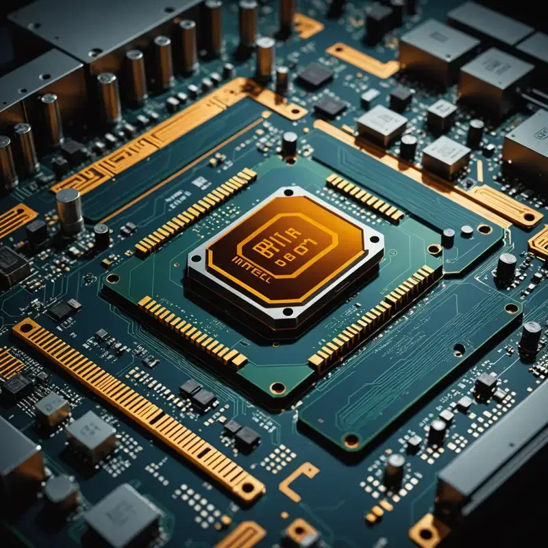
Picture a chip fab the size of several city blocks, running wafers through machines that cost more than a naval destroyer, and the most important announcement coming out of it is nine percent. Not ninety. Nine. That is the number Intel disclosed at the 2026 VLSI Symposium on June 16, and if you understand what it costs to squeeze any performance out of a mature process node, nine percent at the same power level is not a footnote. It is the entire story.
What 'Risk Production' Actually Means Before we talk about
what 18A-P delivers, let us talk about the phrase Intel and the trade press keep using: "risk production," also called test production. According to Intel's official newsroom disclosure at the VLSI Symposium, 18A-P has entered this stage while meeting the timeline Intel previously shared with customers. Risk production is the phase where a fab commits real silicon, real masks, and real tool time to a new process before yield is fully proven. Think of it like a film director shooting the climactic scene before the script is locked: you are spending serious money to find out what breaks. The fact that Intel announced this milestone at VLSI, one of the semiconductor industry's most technically rigorous conferences, rather than at a marketing event, matters. Engineers present papers at VLSI. Marketing teams hold keynotes. This disclosure landed in the engineering room. The educational point here is that semiconductor development has named phases for a reason. A process node that exists only in simulation is a paper promise. One in risk production has physical wafers you can probe, measure, and fail productively. Reaching this stage on schedule, as Intel Foundry stated at the symposium, is a meaningful checkpoint in a multi-year journey from lab to volume manufacturing. Technology Org also confirmed the risk-stage entry, underscoring that this is a verifiable production milestone, not a roadmap slide.
The Numbers They Did Mention, and
the One That Changes Everything The headline figure is the one The Elec reported on June 18: 18A-P delivers a 9% performance increase at the same power level compared to the original 18A process. That is the iso-power comparison, meaning neither node is given a power budget advantage. But WCCFtech's reporting on Intel's pre-VLSI briefing surfaces a second figure that reframes the whole picture: if you flip the optimization and hold performance constant instead of power, 18A-P achieves 18% power savings versus 18A. Those two numbers are two sides of the same PPA (power, performance, and area) envelope. You can cash the improvement as speed, or as battery life, or as heat reduction. The choice belongs to the chip designer. This is a concept worth understanding deeply. Every process node ships with a PPA curve, and a P-suffix variant like 18A-P is essentially Intel tuning where that curve peaks. The original 18A is optimized for a particular balance. The 18A-P shifts the curve toward higher performance headroom while preserving design rule compatibility with 18A, so foundry customers do not have to re-tape-out their chips from scratch. That last detail, confirmed by Intel's newsroom, is significant: a compatible design rule set means existing 18A designs can migrate to 18A-P without starting over.
The Thermal Story Nobody Led With
Here is the spec buried in the briefing that changes the foundry conversation entirely. WCCFtech reported that 18A-P improves thermal conductivity by 50% compared to 18A. Thermal conductivity is not a glamorous spec. It does not show up in consumer benchmark charts. But for a foundry trying to win designs from hyperscalers running data center chips at sustained high loads, it is the spec that determines whether a chip throttles under pressure or holds its performance floor. Thermal throttling is not a graceful degradation. It is the chip breaking a promise it made at the datasheet level, quietly, after the purchase order is signed. Tom's Hardware's reporting adds another dimension: Intel is also pointing to tighter skew corners as a differentiator for foundry customers. Skew corners describe how much a manufactured transistor's characteristics can vary from the ideal. Tighter corners mean more predictable silicon, which means design teams can push closer to theoretical performance limits without leaving as much guard-band margin on the table. For learners new to process engineering, this is a window into why two chips built on nominally the same node can behave very differently in the real world. Process control is not a footnote. It is what separates a yield number from a business.
Why This Matters
for Intel Foundry's Competitive Position Intel's foundry ambitions have been a subject of serious scrutiny for several years. The company is competing with TSMC and Samsung for external chip design customers, and those customers have options. According to Intel's newsroom announcement from June 16, 18A-P is described as the first performance enhancement in the Intel 18A family, and its on-schedule entry into risk production is presented as a signal that the foundry roadmap is advancing against committed customer timelines, not just internal targets. WCCFtech's analysis frames 18A-P as specifically tuned to attract external foundry customers, noting that Intel's original 18A is already ramping for in-house chips like Panther Lake. The 18A-P variant is the version Intel is showing to the outside world: here is what your chip could look like if you trusted us with your wafers. The 50% thermal conductivity improvement and tighter skew corners are not incidental; they are the kind of specifications that show up in procurement decisions at companies building chips that run continuously at high power envelopes. For anyone learning about the semiconductor industry, this moment is a useful case study in what foundry competition actually looks like. It is not just about who has the smallest node number. It is about yield maturity, design support, on-schedule delivery, and whether the process characteristics match the real-world demands of the customers you are trying to win. Intel just put a data point on the board that is measurable, verifiable, and on time. In an industry where the gap between announcement and silicon is often measured in years, that is worth understanding. Watch for how quickly Intel transitions 18A-P from risk production toward volume readiness, and whether external tape-out announcements follow. That is the next milestone that will tell us whether this is a trajectory change or a single good quarter.