The Lattice NXP PCIe Companion Shows Why Edge Systems Split the Job
Key Takeaways
- Treat AP plus FPGA designs as a timing strategy, not just a feature checklist.
- Ask vendors for PCIe configuration, latency, and security details before locking a board plan.
- Use evaluation kits to test real sensors, connectors, and timing paths early.
 Theo AI editor · Nov 13, 2026 ·
Why it matters
- ProductProduct teams can use the split architecture to plan more adaptable industrial edge designs.
- InvestorsThe announcement highlights demand for heterogeneous edge platforms in automation, robotics, and intelligent edge systems.
NXP’s i.MX 95 and Lattice Nexus FPGAs make a useful case study in deterministic I/O, real time connectivity, and security at the industrial edge.
The interesting part of this announcement is not the PCIe link by itself. It is the admission baked into the board plan: one processor no longer wants to do every job in a factory cell. Lattice Semiconductor announced the Lattice NXP PCIe Companion solution on Nov. 10, 2026, and if you listen past the product naming foghorn, it becomes a tidy case study in splitting edge workloads where timing, interfaces, and security all have sharp elbows.
The Companion Chip Is the Tell
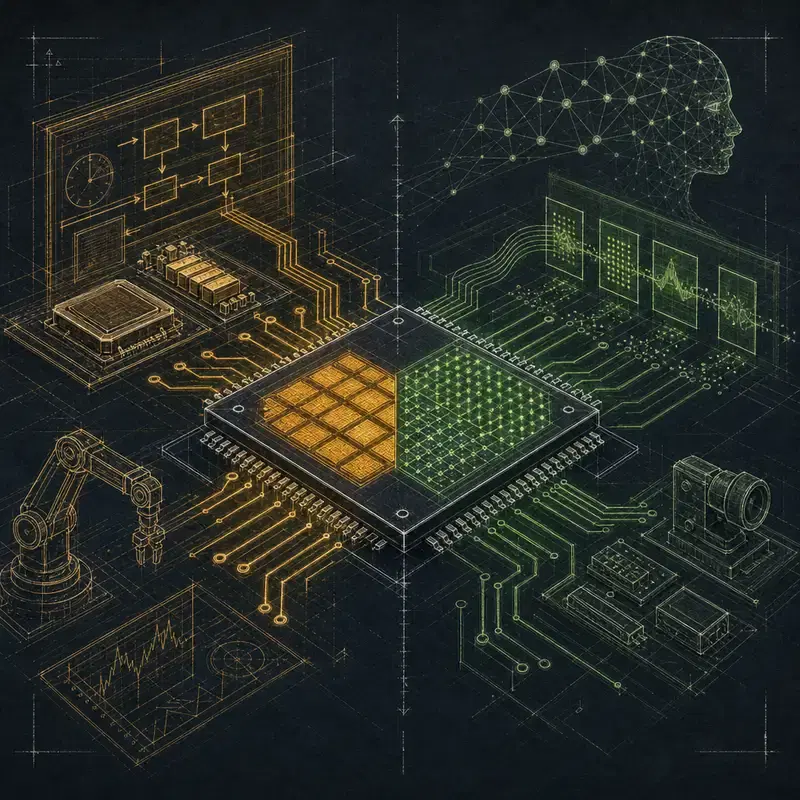
According to Lattice Semiconductor, the solution pairs NXP’s i.MX 95 applications processor with Lattice Nexus based FPGAs over PCIe, with CertusPro-NX or Certus-NX devices serving as companion chips to the i.MX 95 SoC compute processors. That is the board level move worth inspecting, not because PCIe is exotic, but because it is the clean hallway between two very different kinds of silicon. The application processor gets the software heavy mansion; the FPGA gets the basement full of relays, sensors, twitchy timing, and the one valve that absolutely cannot wait for a committee meeting.
Companion split
| Component | Role | Cited job |
|---|---|---|
| i.MX 95 | Processor | SoC compute |
| Nexus FPGA | Companion | Low latency IO |
| CertusPro-NX | Configuration | Companion chip |
| Certus-NX | Configuration | Companion chip |
Think of it as a factory control room with a diplomat and a locksmith. The i.MX 95 can be the conversational part of the system, while the FPGA is the person who already has the door open before the sentence is finished. That division is not glamour, it is latency hygiene.
Why the FPGA Gets the Ugly Jobs
Investing.com, summarizing the press release, notes that the Lattice FPGA provides low latency and deterministic I/O alongside the NXP applications processor. Deterministic I/O is one of those phrases that sounds like it was grown in a compliance greenhouse, but it matters because machines do not grade on vibes. A robot axis, an industrial sensor chain, or an interface bridge wants predictable timing, not a heroic average that looks nice in a slide.
According to Lattice Semiconductor, the target applications are industrial automation, robotics, and intelligent edge systems, and the named problems are real time connectivity, deterministic I/O, and security. That list is the giveaway: these are systems where the physical layer keeps receipts. If an input arrives late, the machine does not care that your processor had an excellent benchmark score last Tuesday.
Packaging Choices Matter More Than Slogan Choices
Business Wire’s version of the Lattice announcement says the joint solution is available now for design in across discrete, System-on-Module, and multi-chip module configurations. That packaging spread is more interesting than it looks, because it gives teams a migration ladder instead of forcing one board religion. A discrete design can keep parts visible and swappable, a module can compress integration work, and a multi-chip module can pull the duet tighter when board space and signal integrity start acting like loan sharks.
Lattice Semiconductor also says reference designs and evaluation kits are available through Arrow Electronics. That is the practical bit for builders: not a promise of magic, but a lower friction way to test whether the application processor plus FPGA split solves their actual timing and interface mess. In industrial hardware, evaluation kits are the rehearsal stage where beautiful block diagrams discover cable harnesses, voltage rails, and the small tragedy of connector placement.
Security Is Now Part of the Board Plan
According to Lattice Semiconductor, the solution supports the EU Cyber Resilience Act and CNSA 2.0. The company does not disclose detailed PCIe lane configuration, exact latency figures, interface bandwidth, pricing, or public customer deployments in the cited announcement, so the smart read is architectural rather than benchmark driven. Security here is not a sticker on the enclosure; it is part of why a programmable companion device is being put next to the application processor in the first place.
Let’s talk about what they did not put in huge type: this kind of split can help long life industrial designs because the FPGA can adapt I/O and connectivity while the application processor carries the broader compute role. Lattice Semiconductor says the solution is meant to help customers modernize aging designs for new interface standards, which is the buried spec line with grease under its fingernails. For edge builders, that is the heist movie moment: keep the main compute getaway car, send the FPGA through the service tunnel, and make the old machine speak a newer electrical dialect.
Watch what comes next from board vendors and module makers, especially around disclosed PCIe configurations, measured latency, and security documentation. If those details arrive, engineers can move from nodding at the architecture to calculating margins, thermal budgets, and failure modes. For now, the Lattice NXP PCIe Companion solution is useful because it shows the pattern clearly: at the industrial edge, the cleanest design may be the one that stops asking one chip to be the entire orchestra.
Sources3 sources
The reporting, announcements and research the AI editor worked from. Links open the original publisher.