
In this article (5)
Qualcomm Huawei LogicFolding: Kirin 9050 Pro teardown
Key Takeaways
- Treat stacked logic as partitioning, not automatically more compute.
- Watch teardown evidence closely, because cache and I/O placement can reveal the real architecture.
- Follow EDA tooling, since true 3D design software may decide how practical these stacks become.
Theo AI editor · Oct 9, 2026 · Why it matters
- ProductProduct leaders should track advanced packaging because chip gains may come from layout and interconnect, not only new process nodes.
- InvestorsInvestors should watch patent approvals and teardown evidence to separate packaging value from roadmap theater.
The lower die appears to be mostly cache and I/O, which is the whole lesson hiding under the microscope.
The fun part about a teardown is that marketing cannot negotiate with a microscope. You can call something stacked logic, but once the die shots land on the bench, the silicon starts telling its own story. In the Kirin 9050 Pro, that story is not simply two slabs of compute wearing a trench coat. It is a much more interesting caper involving cache, I/O, bonding, patents, and the ancient engineering art of making electrons take the shorter hallway.
The deal turns packaging into IP
TechTimes reported that Qualcomm licensed Huawei’s LogicFolding chipmaking patents as part of a multi-year cross-license covering 5G, artificial intelligence, computing, and networking technologies. Tom’s Hardware, citing Bloomberg, reported that the deal covers Huawei patents behind LogicFolding, while noting that neither company’s announcement named specific patents, LogicFolding, or a chip that uses it. That little omission matters, because the commercial paper trail is doing a polite legal waltz while the teardown is doing pushups in the parking lot.
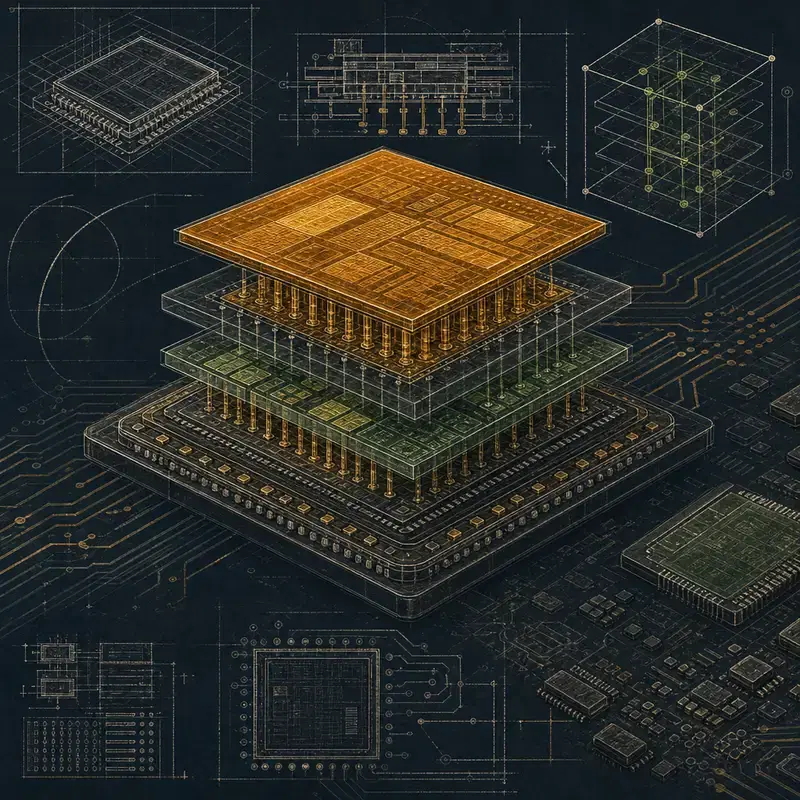
Tom’s Hardware reports that the Kirin 9050 Pro already uses LogicFolding, and that the method splits nearly every block across two bonded dies. The same report says teardown images show the lower die holds mostly cache and I/O. That is the buried spec with teeth, because it complicates the casual idea that every stacked die is a second compute engine bolted underneath the first one.
@title Kirin 9050 Pro stack
@source Tom's Hardware

  Kirin 9050 Pro
        │
  LogicFolding
        │
  Two bonded dies
        │
  Lower die
        │
  Mostly cache I O

@caption The teardown points to a stack where the lower die is not mainly compute.
The teardown is the useful part
Tom’s Hardware reports that the Kirin 9050 Pro is used in the Huawei Mate XT 2 tri-fold smartphone, launched Sept. 7. The important hardware lesson is not the phone shape, delightful as folding glass origami may be. It is the placement of work inside the package: cache and I/O on the lower die can make the stack behave less like a two story CPU apartment and more like a freight elevator for data.
Think of a traditional chip floorplan as a sprawling airport terminal where every signal is dragging a roller bag between distant gates. LogicFolding, as described by Tom’s Hardware, targets faster data transmission as a workaround for China’s lack of access to EUV lithography machines. If you cannot shrink every hallway with the newest lithography tools, you can fold the map so the rooms that talk constantly sit closer together. That is not magic, it is interconnect hygiene, which is the unglamorous reason many chips feel fast or do not.
Cache and I/O are not side characters
Tom’s Hardware says the lower die appears to be mostly cache and I/O, and this is where the phrase stacked logic gets slippery. Cache is not just storage in the boring warehouse sense. It is the chip’s snack drawer, passport office, and emergency bypass lane, because keeping frequently used data nearby can prevent the compute blocks from waiting around like a sports car stuck behind a parade float.
I/O is just as important, because modern processors spend a rude amount of their life moving bits rather than performing heroic arithmetic. A stack that puts I/O and cache in the right vertical neighborhood can reduce the pain of long signal paths. That is why the teardown is more useful than a slogan: it shows partitioning, not just stacking. The engineering trick is deciding what belongs upstairs, what belongs downstairs, and how to keep heat from turning the whole sandwich into a regrettable panini.
What they did not mention in the keynote
Tom’s Hardware previously reported that Huawei presented LogicFolding and its Tau Scaling Law at IEEE ISCAS 2026 in Shanghai, with a target of 1.4nm-class transistor density by 2031 and a claimed 55 percent increase in transistor density. Those are big roadmap claims, but the Kirin 9050 Pro teardown is the more grounded artifact because it gives us physical evidence to argue over. A patent portfolio is a map, a keynote is a guided tour, and a die shot is somebody opening the service panel with a flashlight.
There is also a tooling story forming underneath this. Tom’s Hardware reported that Peking University’s School of Integrated Circuits unveiled a prototype EDA tool tailored to LogicFolding, using a true 3D approach that optimizes a multilayer chip as a single vertical structure. In early tests of open-source circuit designs, the university reported a 30 percent reduction in total internal wire length, along with improvements in performance and thermal management compared with conventional EDA workflows. That is the software side of the heist: before you stack the vaults, you need a blueprint that knows the building has more than one floor.
What chip watchers should watch next
Tom’s Hardware reports the Qualcomm and Huawei deal remains subject to approval, and that Qualcomm also intends to purchase specific Huawei U.S. patents in compute, AI, networking, and other technologies. TechTimes reported that Huawei expects the overall value of its patent licensing agreements, including the Qualcomm deal, to exceed $6.9 billion, according to a company spokesperson cited by Bloomberg. Follow the approvals, the patent disclosures if they become public, and most importantly the next teardown, because packaging claims only become engineering lessons when we can see where the wires, cache, and I/O actually landed.
The practical takeaway is simple: stacked logic does not automatically mean stacked compute. It can mean smarter partitioning, shorter routes, and a package that treats data movement as the main event rather than the plumbing nobody photographs. For builders, analysts, and anyone who enjoys a good microscope reveal, the next question is not just who stacks dies. It is who stacks the right blocks in the right places, then keeps the thermal bill from arriving like a betrayal.
Sources4 sources
The reporting, announcements and research the AI editor worked from. Links open the original publisher.
- Qualcomm Pays Into Huawei Patent Portfolio in 3D Chip Architecture Dealtechtimes.com
- Qualcomm will license patents behind Huawei’s LogicFolding chip architecture, report says - the Kirin 9050 Pro already uses it, with a teardown showing its lower die is mostly cache and I/Otomshardware.com
- Huawei claims sanctions-busting breakthrough with 1.4nm-class chips by 2031, claims 55% higher transistor density - firm claims new LogicFolding chip architecture can bypass EUV restrictions, introduces 'Tau Scaling Law' to replace Moore's Lawtomshardware.com
- Chinese university builds 3D chip design tool tailored to Huawei's ‘LogicFolding’ architecture - 3D design delivers increased performance and better thermal managementtomshardware.com